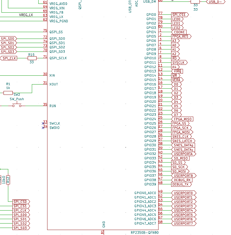
As you can see, I am using ALL the I/O the RP2350B has to offer.
you are viewing a single comment's thread
view the rest of the comments
[–] [S] 1 point 1 day ago (5 children)

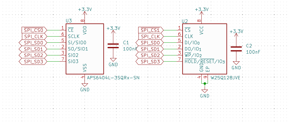
Got your PSRAM and SPI flash ROM right here. The firmware has to boot the RP2350B and contain the bitstream for the FPGA, which gets loaded via bit-banging SPI on its own four pins.
None

  • source
  • parent
  • hideshow 5 child comments
  • [–] [S] 1 point 1 day ago (4 children)

    Stupid simple power supply: USB-C +5V, 15W. Way more than anything on this board needs anyway. Little 3.3V regulator for the I/O, 1.2V for the FPGA.I could have run the 1.2V over to the MCU to replace the fiddly switching power supply, but I worry that doing that will hamper overclocking.

    None

  • source
  • parent
  • hideshow 4 child comments
  • [–] [S] 1 point 1 day ago (3 children)

    VERA outputs VGA via a simple resistor DAC. Nothing special here.

    None

  • source
  • parent
  • hideshow 3 child comments
  • [–] [S] 1 point 1 day ago (2 children)

    A DAC for the I2S audio from VERA outputs line-level stereo. This part I know works. It's lifted from Sentinel 65X.

    None

  • source
  • parent
  • hideshow 2 child comments
  • [–] [S] 1 point 1 day ago (1 child)

    User port and debug serial port, plus the two SNES controller ports (not shown) round out the system.Not much to it really. The magic is all in the firmware.

    None

  • source
  • parent
  • hideshow 1 child comment